Product description
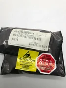
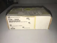
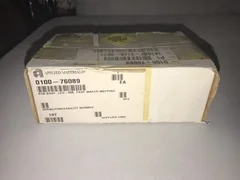
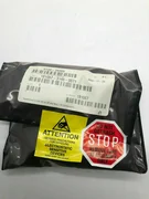
LED-WB fast wafer-mapping PCB assembly used in wafer mapping or wafer-detection hardware.
Specifications and identifiers
Control context
| Likely subsystem | Fast wafer mapping References consistently associate the board with fast wafer mapping, but exact platform should be verified. |
|---|
Identification
| Functional item | PCB assembly, LED-WB, fast wafer mapping A board assembly related to LED-based wafer mapping or detection. |
|---|
| Board function | Wafer mapping illumination/detection support LED wafer-mapping boards are commonly used to help detect wafer presence or slot position in handling modules. |
|---|
Equipment context
- Applied Materials wafer-handling or mapping subsystem
Applications
wafer mappingload lock or cassette mappingwafer-handling diagnosticsLED sensor board replacementwafer mapping board replacementLED wafer-detection repairwafer-handling sensor troubleshootingload lock/cassette mapping service
How it works
A wafer-mapping LED PCB is an electronics board used in an optical or LED-based wafer-detection/mapping subsystem.
Wafer mapping helps verify wafer presence, slot position, and handling status; board failure can cause mapping errors or robot transfer faults.
Technical guide
LED printed circuit board
A PCB populated with LEDs and interface electronics.
LED output, board alignment, connector condition, and revision can affect mapping accuracy.
Verify: LED function; connector condition; revision; mounting alignment; board cleanliness
optical wafer mapping
A wafer-detection method using light emitters/sensors to identify wafer presence or slot position.
Accurate mapping prevents wafer-handling collisions, mis-picks, and cassette/load lock errors.
Verify: emitter/sensor alignment; LED wavelength or intensity if specified; board revision; controller compatibility
- LED
- Light-emitting diode.
- PCB
- Printed circuit board.
- WB
- Likely wide beam or board-specific designation; verify from tool documentation.
What to verify before purchase
- Confirm the exact LED-WB board variant and revision.
- Verify connector layout, mounting location, and optical alignment requirements.
- Check LED output, board cleanliness, and signs of ESD or handling damage.
- Confirm the target tool or wafer-handling module from the service manual.
Confirm with the seller
- Exact Applied Materials platform
- LED wavelength/intensity specification
- Board revision
- Controller compatibility
Product reference only. Confirm fitment, revision, included components, and specifications before purchase.