Product description
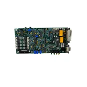
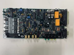
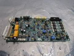
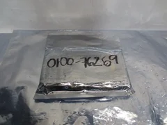
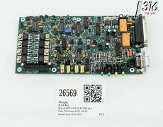
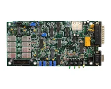
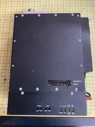
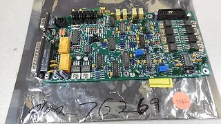
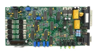
RF match control PCB / PCBA control board for Applied Materials RF matching equipment.
Specifications and identifiers
board context
| Assembly form | PCBA / control board A populated printed circuit board used for control logic or interface functions. |
|---|
identification
| Function | RF match control PCB Control electronics associated with an RF matching network. |
|---|
| Board reference | 07031514-1 An alternate board marking or vendor/reference number identified with this assembly. |
|---|
Applications
plasma etch chambersPVD/CVD plasma systemsRF generator-to-chamber matchingRF match control electronicsplasma chamber RF subsystem repair
How it works
An RF match network or RF match control component used to couple RF power efficiently into a plasma load.
Frequency, power rating, impedance range, connector layout, and chamber-specific tuning requirements are critical for plasma process stability.
Technical guide
rf_power
RF power systems often use generators, matching networks, and interlocks to stabilize energy delivery to a chamber.
- PCB/PCBA
- Printed circuit board / printed circuit board assembly.
- RF
- Radio frequency; in plasma tools this commonly refers to power used to generate or bias plasma.
What to verify before purchase
- Board revision and firmware/configuration
- Connector layout and installed components
- Matching RF match network assembly
Confirm with the seller
- RF frequency or power rating of the complete match system
Product reference only. Confirm fitment, revision, included components, and specifications before purchase.