Product description
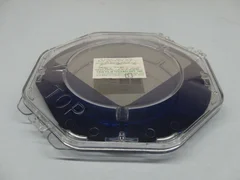
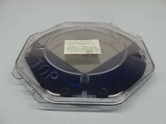
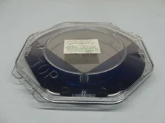
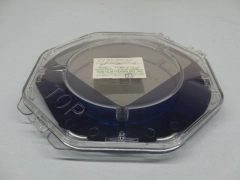
Laser alignment wafer, 150 mm, Rev A context
Specifications and identifiers
supported identity
| Item type | Laser alignment wafer A wafer-shaped alignment tool used for optical/mechanical alignment. |
|---|
| Wafer size | 150 mm Size appears in both supporting source titles. |
|---|
| Revision context | Rev A Revision should be checked on the item. |
|---|
Applications
wafer handlingload-lock safetyprocess endpoint detectiontool alignmentTool alignmentWafer path or optical alignment checksService/calibration support
How it works
A laser alignment wafer senses, detects, or indicates a physical condition such as wafer presence, pressure, endpoint, or alignment.
Sensors and detector modules support interlocks, automation, process monitoring, and calibration.
Technical guide
common
Sensor assemblies may include optics, switches, electronics, cables, and mounting brackets.
sensing
Semiconductor tools use sensors to confirm safe states and process conditions.
- ATM
- Atmosphere or atmospheric pressure context.
- endpoint
- A detected process condition used to determine process completion.
What to verify before purchase
- Confirm wafer diameter, revision, and whether it contains active or passive alignment features.
- Inspect for chips, scratches, or contamination.
- Verify calibration or service status if required.
Confirm with the seller
- Exact alignment method and calibration status are not confirmed.
Product reference only. Confirm fitment, revision, included components, and specifications before purchase.