Product description
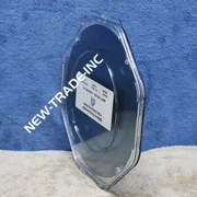
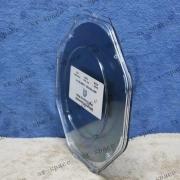
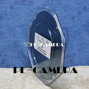
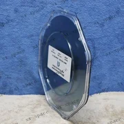
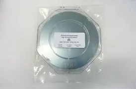
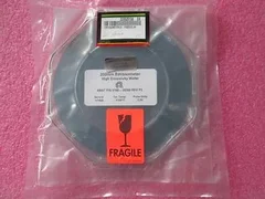
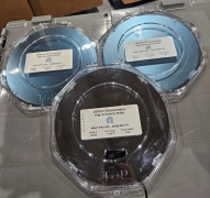
8 inch / 200 mm emissometer high-emissivity test wafer.
Specifications and identifiers
metrology details
| Component | High-emissivity wafer Supported descriptions identify a high-emissivity test wafer. |
|---|
| Size | 8 in. / 200 mm Both equivalents appear in supported wording. |
|---|
| Use | Emissometer / test wafer Likely used for emissivity/thermal measurement checks. |
|---|
Applications
Lithography steppers/scannersMicroscope systemsLaser-axis measurementWafer measurement and mappingThermal/emissivity measurement referenceTool calibration or process metrology check
How it works
An optical or metrology component supports imaging, measurement, alignment, or light-based inspection functions.
Optical alignment, wavelength compatibility, calibration state, and cleanliness can be essential to measurement accuracy.
Technical guide
common
May include optical glass, sapphire, lenses, mirrors, mounts, or precision electronics.
optical measurement
Uses light, imaging, or interferometry-style measurement hardware.
What to verify before purchase
- Verify wafer condition, coating/emissivity surface, serial/lot, and whether it is intact and cleanroom-packaged.
Confirm with the seller
- Exact emissivity value and calibration status are not confirmed.
Product reference only. Confirm fitment, revision, included components, and specifications before purchase.