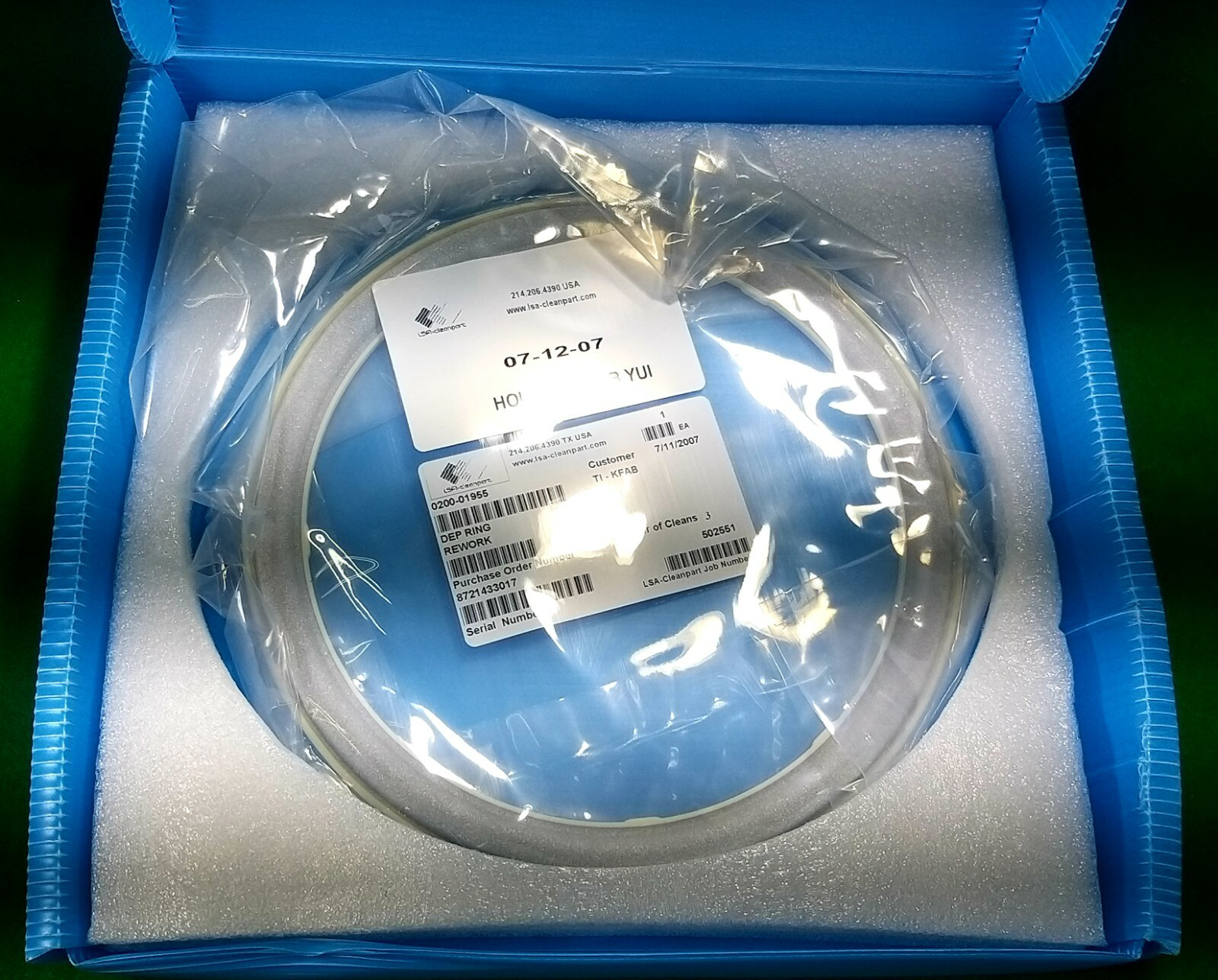
Product description
Deposition ring for 200 mm SIP Ta/TaN / SNNF ESC PVD context; one source also references Al2O3/Kachina wording.
Specifications and identifiers
details
| Wafer size | 200 mm |
|---|
| Process context | SIP PVD / Ta-TaN |
|---|
| Associated hardware | SNNF ESC mentioned |
|---|
identification
| Normalized item type | Deposition ring |
|---|
| Supported description | Deposition ring for 200 mm SIP Ta/TaN / SNNF ESC PVD context; one source also references Al2O3/Kachina wording. |
|---|
Applications
PVD/CVD/etch process chamberselectrostatic chuck assembliesdeposition shields, liners, rings, and coversPVD chamber edge/deposition shieldingReplacement ring for 200 mm deposition hardware
How it works
A chamber or wafer-processing hardware component used around the wafer, chamber wall, source area, or electrostatic chuck stack.
Geometry, material, coating, and wafer size strongly affect process fit, plasma exposure, and contamination control.
Technical guide
ceramic_or_metal
Many chamber parts use ceramics, aluminum, stainless steel, quartz, or coated metals depending on plasma and chemistry exposure.
ESC
Electrostatic chuck hardware clamps or supports wafers during processing.
What to verify before purchase
- Confirm material/coating variant: Ta/TaN versus Al2O3 wording.
- Confirm cleaned/refurbished/new condition and chamber family.
Confirm with the seller
- Exact machine compatibility beyond the named platform/context is not confirmed.
Product reference only. Confirm fitment, revision, included components, and specifications before purchase.