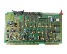
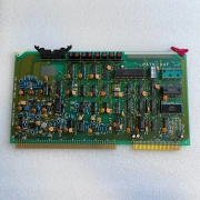
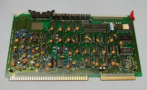
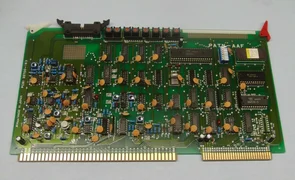
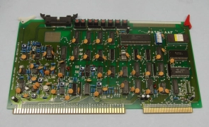
Product description
PCB1 auto focus CCD control board, 2-PAT-V 3.63 / PATN-AAF context
Specifications and identifiers
identified attributes
| Board function | Auto focus CCD control Controls or interfaces with CCD/autofocus function. |
|---|
| Board identifier | PCB1 / 2-PAT-V 3.63 / PATN-AAF Identifiers appear in supported descriptions. |
|---|
| Generic alternate | PCB interface / circuit board Some descriptions use more generic wording. |
|---|
Applications
tool control electronicsI/O expansionfieldbus interfacesembedded computer/control racksNikon autofocus/imaging electronicsCCD control board replacementmicroscope or inspection tool service
How it works
A printed circuit board or electronic module used for control, interface, communication, sensing, or computing functions inside semiconductor equipment.
Board revision, firmware, bus type, and connector configuration are often critical for compatibility.
Technical guide
PCB
Fiberglass/epoxy printed circuit substrate with copper traces and mounted electronic components; exact board stackup is not confirmed.
I/O
Input/output electronics interface sensors, actuators, fieldbus devices, or other tool modules.
- I/O
- Input/output
- PCB
- Printed circuit board
- PCBA
- Printed circuit board assembly
- RS-232
- Serial communication standard
- RS-485
- Industrial serial communication standard
- VME
- Versa Module Europa bus
- cPCI
- CompactPCI
What to verify before purchase
- Verify exact PCB revision and PATN/2-PAT-V marking.
- Confirm microscope/tool model compatibility.
Confirm with the seller
- Exact Nikon instrument model is not confirmed.
Product reference only. Confirm fitment, revision, included components, and specifications before purchase.